Package Conventions
|
These guidelines are not yet complete. Help us create sensible conventions on GitHub! |
Scope
The most important thing to consider when creating a package is the scope of it. Since LibrePCB handles footprints differently than other EDA tools, special attention is required here.
Think about the appearance of the part (the mechanical shape, dimension and color). If two parts look exactly (or almost) equal, they can use the same package. If they look different, two separate packages must be created.
|
Don’t think about the land pattern (i.e. footprint) of the part — it’s not relevant for this decision. Even if a package can be mounted differently on a PCB (e.g. a THT resistor can be mount horizontally or vertically) and thus require different footprints, only one package is needed. Similarly, two different-looking parts that have the same land pattern (e.g. a SMD resistor and a SMD LED) should still be two separate packages. |
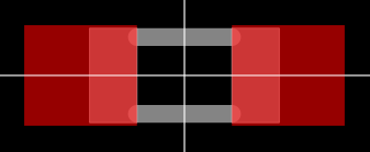
Even if a 0805 LED with a transparent lens has exactly the same footprint as a 0805 LED with a red lens, they should have separate packages because of the different color. This way a device can link to the package with the proper color, and thus it will appear with the proper color in the 3D PCB preview (once LibrePCB supports 3D models).
Some packages are available in different heights. For instance, SO-8 is available with heights of 1.2mm and 1.4mm. As the 3D models would be different, separate packages are needed.
Note: To avoid creating too many packages, a small tolerance is allowed. So for a device with a height of 1.3mm you might want to use the package with a height of 1.4mm.
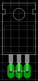
Many packages can be mounted either vertically or horizontally, for example the TO220. If mounted horizontally, there might be a hole in the PCB to screw the metal tab down to the PCB, or you may want to solder the tab to the PCB without a hole in it. For all these cases only one package is needed — the different mounting variants should be handled by different footprint variants inside the package.
Naming
The following conventions apply to package names:
-
We generally follow IPC-7351 when naming packages (e.g. "SOT23-5P95_280X145L60" instead of "SOT23-5"). Alternative names (like "SOT23-5") should be added to the comma-separated keywords list and maybe to the description.
-
For packages not covered by IPC-7351, use following naming conventions:
-
Language must be American English (en_US), if applicable (many packages have language-neutral names anyway).
-
Size information must use metric units, not imperial units.
-
For packages which are available with different pin counts, append the pin count with a hyphen as separator and omit leading zeros (e.g. "DIP-8" instead of "DIP08").
-
-
For packages which are well known by their size in imperial units (e.g. "0805" which is "2012" in metric), it’s recommended to write the well known name in parentheses. For example, a chip resistor could be named "RESC2012X70 (0805)".
-
The name of manufacturer-specific packages should start with the manufacturers name in capital letters, followed by an underscore (e.g. "MOLEX_53261-06"). The Library Expert naming conventions contain concrete recommendations for many manufacturers, please follow them. Note: Libraries do not act as namespaces for package names, so you should start the package name with the manufacturers name even if the package is located in a manufacturer-specific library.
Pads
-
Each lead of the package should be represented by a separate package pad, even if there are internal connections (e.g. multiple GND leads) or unconnected leads (e.g. the often unused metal tab of a TO220). Exceptions:
-
Multiple mechanical leads which have a package-internal connection (e.g. tabs of the metal housing of an USB connector) should be represented by a single package pad (and all footprint pads connected to it).
-
Leads for pure mechanical purpose without any internal connection at all (e.g. split solder tabs of a plastic connector) shouldn’t be added as package pads (the corresponding footprint pads can be left unconnected). If in doubt or if connected to a metal cover of significant size (possibly having a shielding function), treat them like normal, electrically relevant leads.
-
-
Use pad names according IPC-7351 (if applicable). For packages which are not covered by IPC-7351:
-
If the function of a pad is absolutely clear, choose its abbreviated functionality as name (e.g. "A" for anode and "C" for cathode).
-
Otherwise just use numbers starting with "1" at top left and increment them counterclockwise.
-
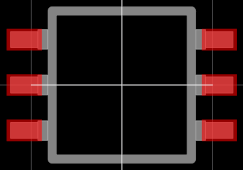
Footprints
Within a package there can be multiple footprint variants. They are intended to support the following use-cases:
-
Mounting variants: For example, a THT resistor can be mounted either vertically or horizontally with various pad distances. Every common mounting variant should be available as footprint variants.
-
Soldering techniques: Many packages can be soldered either by reflow-, wave- or hand-soldering, which usually require different land patterns. For every suitable soldering technique there could be a corresponding footprint variant.
-
Density levels: IPC-7351 specifies three different density levels for footprints:
-
Density Level A: Maximum (Most) Land Protrusion
-
Density Level B: Median (Nominal) Land Protrusion
-
Density Level C: Minimum (Least) Land Protrusion
If applicable, these three density levels should also be added as footprint variants.
-
|
Combinations
As a given package might support multiple of the use-cases above, all suitable combinations of them should be added. For example a package which should have all three density levels as defined in IPC-7351 and can be mounted either vertically or horizontally would need six footprint variants to support all possible use-cases. |
|
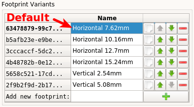
Set default footprint
The first footprint is always the default footprint, so you should move the most reasonable footprint to the top of the footprint list! The default footprint should fulfill these rules:
|
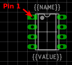
Origin
The origin (0, 0) should be exactly at the center of the package body. It is used by pick and place machines.
Some packages (especially those with non-symmetrical body) have the origin explicitly specified in the datasheet. In that case, use the origin from the datasheet.
Orientation
Footprints must be drawn from the top-view. When a footprint needs to appear on the bottom of a board, this can be done in the board editor by mirroring it.
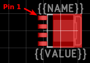
Pin 1 should always be at the top left, as defined in IPC-7351C "Level A", slide 22.
Legend Layer
|
In LibrePCB 0.1.x, these layers were called Top/Bottom Placement. Starting with LibrePCB 1.0, they are now called Top/Bottom Legend. |
The Top Legend layer is intended to be printed on silkscreen and thus should contain information required for assembling the PCB. But don’t put too many things on that layer as it would waste space on the PCB!
Typically this layer should only contain some lines and dots to indicate where and in which orientation the device gets assembled, for example an outline and a dot next to pin 1.
The legend should be drawn according to IPC-7351C. The most important rules are the following:
-
It should stay visible after assembling the package to allow reviewing positioning and orientation of assembled devices. In other words, the legend layer should primarily contain drawings around the package’s body, but not under it.
-
Line width: 0.2mm typical, 0.1mm minimum
-
Clearance to copper layers: Equal or greater than the line width, but at least 0.15mm
Documentation Layer
The layer Top Documentation should be used to draw the most important details of the package’s appearance. It could be considered as an alternative to the 3D model of a package. But in contrast to the 3D model, the documentation layer is visible in the board editor while layouting the PCB.
Following things should be placed on the documentation layer:
-
The package’s exact outline. Attention: The outer edges of the lines should correspond to the package’s edges, not the middle of the lines! So, for example if the body is 5x5mm and the line width 0.2mm, you have to draw a 4.8x4.8mm rectangle.
-
The top view of the leads/legs: The leads or legs of both THT and SMT pads should be drawn from the top view, i.e. the vertical projection of them. This is needed to make packages look realistic on the documentation layer, as leads and legs are an important part of the appearance of packages.
-
The contact area of SMT leads: The area where SMT leads touch the copper land pattern should be drawn as filled polygons with a line width of 0mm. This helps the PCB designer to see the expansion of the land pattern, i.e. how much copper is around the actual lead.
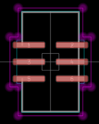
Package Outlines Layer
Every typical footprint should contain a single polygon on the Top Package Outlines layer to specify the outer dimension of the package. It is used by the DRC to check the clearance between devices.
General rules:
-
Any leads shall be included, but pads not.
-
Line width: 0.0mm
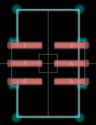
Courtyard Layer
Every typical footprint should contain a single polygon on the Top Courtyard layer to specify the area where no other device shall be placed. It is used by the DRC to check this requirement. Usually this is equal to the Package Outlines Layer, just with an offset of several 0.1mm.
General rules:
-
Line width: 0.0mm
-
Offset to outlines: According to IPC 7351 if applicable. A typical value for SMT devices is 0.2mm. For THT devices, a larger value (e.g. 0.4mm) is recommended.
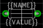
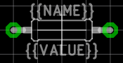
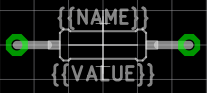
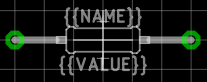
Text Elements
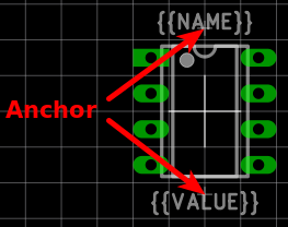
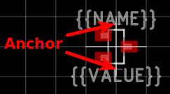
Typical footprints should have exactly two text elements: {{NAME}} and
{{VALUE}}.
The name should normally be placed at top of the package body, slightly above the outline and aligned at bottom center. The value should be placed at the bottom center, slightly below the package body and aligned at the top center.
Always make sure that the text elements do not overlap with pads or with the placement layer. Otherwise the text might be unreadable on silkscreen. In addition, text elements should usually be placed outside the package body to still see them on silkscreen of an assembled PCB.
Keep in mind that the bottom-aligned anchor is placed on the text baseline. This means that some letters like "g" or "y" might extend slightly below the anchor.
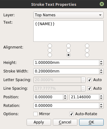
| Property | Name text element | Value text element |
|---|---|---|
Layer |
Top Names |
Top Values |
Text |
{{NAME}} |
{{VALUE}} |
Alignment |
Bottom Center |
Top Center |
Height |
1.0mm (or larger) |
1.0mm (or larger) |
Stroke Width |
0.2mm (or thicker) |
0.2mm (or thicker) |
Letter Spacing |
Auto |
Auto |
Line Spacing |
Auto |
Auto |
Mirror |
No |
No |
Auto-Rotate |
Yes |
Yes |
|
Special cases
These rules should be fine for many packages, but probably not for all of them. For special cases it’s allowed to have slightly different properties if they are more suitable. |
3D Models
Packages might be populated with 3D models from STEP files. However, there are several things to consider carefully.
Some general notes:
-
File size: Try to keep STEP models as small as possible to avoid unnecessary long download- and loading times. Usually it is fine to keep STEP models rather simple (i.e. not adding too much details).
-
License: Keep in mind that all libraries provided by LibrePCB are released under the CC0 Public Domain license. This also applies to STEP models.
|
Almost every STEP model available in the Internet (whether from a manufacturer or some other website) are not published under the CC0 license and sometimes are also very bloated (way too detailed). Such models must not be contributed to our official libraries (we won’t accept them). We may change this requirement some day, but at the moment this needs to be respected. In addition, we prefer STEP models to be generated with CadQuery to allow making modifications in future. Contributions of STEP models created in any other way may not be accepted. |