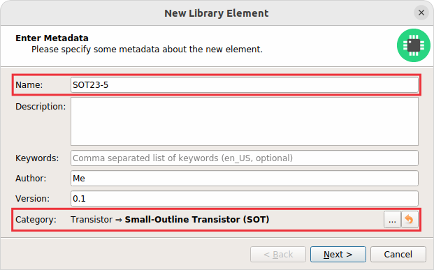
Package
Then you need to create the package for the LMV321LILT, which is called SOT23-5. As usual, click New Package and specify the name and category of the new package. In addition, it’s recommended to also specify the assembly type, i.e. whether this is a through-hole (THT) or surface-mount (SMT) device:
Add Pads
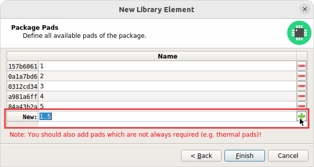
Now you need to specify all pads of the package. The SOT23-5 has 5 pads named from 1 to 5, so you can just enter the term 1..5 and click on the + button (or press Return):
|
When adding the pads, don’t consider their electrical functions or internal connections. For example if a transistor with three electrical signals has three pads plus a thermal pad connected to one of the other signals, the package has four pads in total. It’s not relevant whether some of them are connected to each other within the package. General rule of thumb: If in doubt, better specify too many pads than too few ;-) |
Place Pads
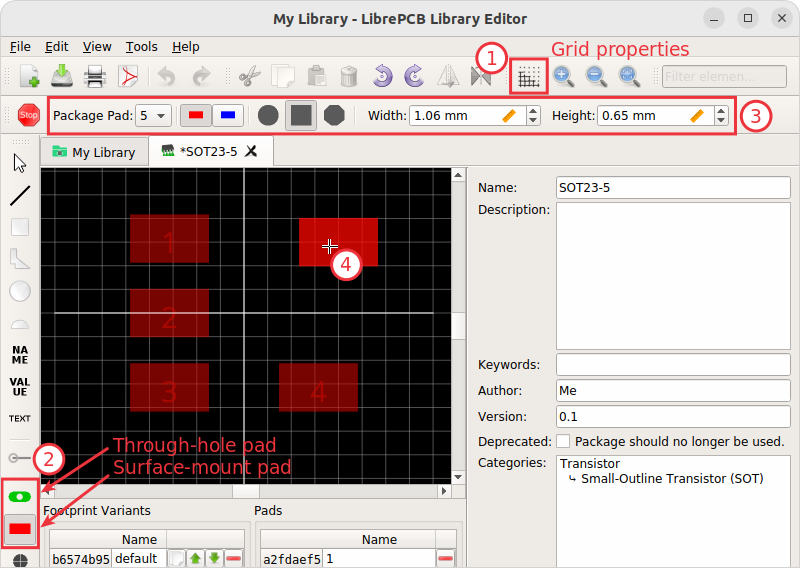
After clicking on Finish, you can draw the footprint. It’s recommended to start with placing the pads:
-
Set a reasonable grid interval in the status bar, if desired. You can either press F4 and type in the new interval, or hover with the mouse on the number and scroll up or down to change the value.
-
Start either the Add THT Pad or Add SMT Pad tool.
-
Choose the package pad to place and specify its properties, most notably the shape and size.
-
Place the pad with a click. Press R to rotate it while moving.
|
The tool only allows to place pads on the grid. To specify exact coordinates, just place the pads rougly and open Properties from the pad’s context menu (right-click) afterwards to enter exact values. |
Draw Polygons
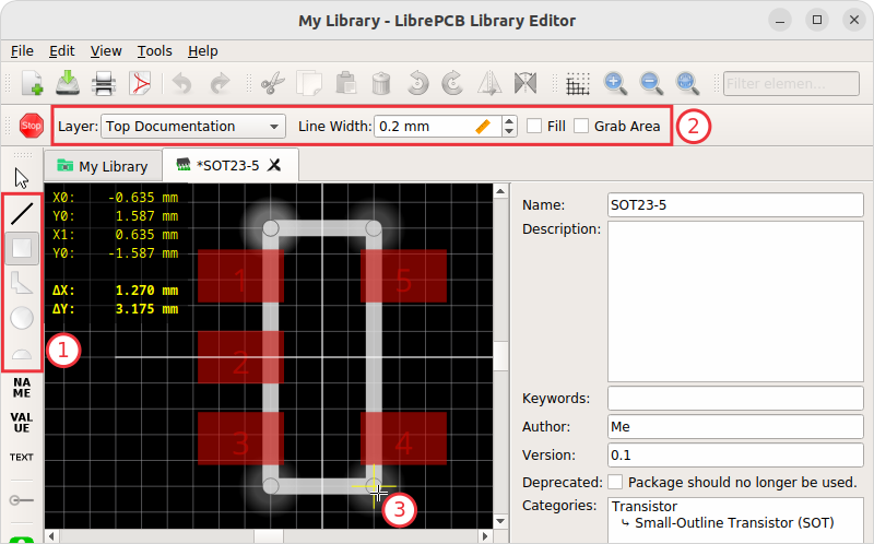
Then add graphical object just as done in the symbol editor:
|
It’s recommended to add at least two polygons:
To create highly functional, beautiful looking footprints, check out our package conventions. |
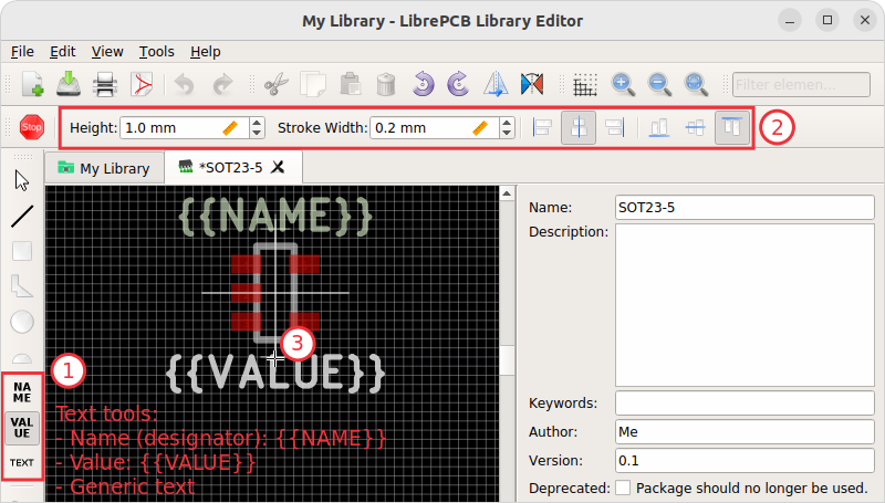
Add Texts
Just like in the symbol,
you should add {{NAME}} and a {{VALUE}} text objects:
Add Non-Plated Holes
In case your package requires to drill non-plated holes into the PCB (for example to insert a screw), use the Add Hole tool and specify its diameter. However, for our SOT23-5 package we don’t need a hole.
That’s all you need for a simple package! Now save the package to ensure the background library scan picks up the new package.
Add 3D Model
If you have a STEP file of the package, you can add it as a 3D model to the package. Switch to the tab 3D Models (Ctrl+3) and click on the + button to import the STEP file (this may take a while):
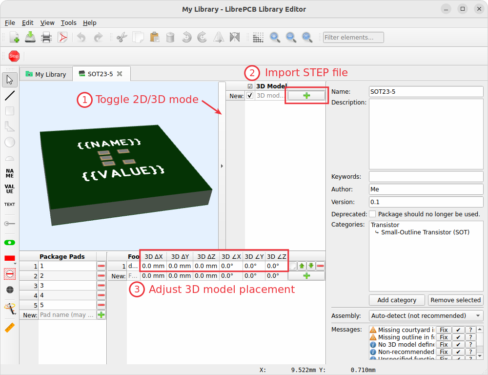
If required, the position and rotation can be adjusted at the bottom right (note that Return needs to be pressed to accept new values).
Recommendations
For details about how packages should be designed, please take a look at our package conventions. The most important rules are:
-
Create generic packages, not specific ones. For example DIP08 is DIP08 — no matter whether it’s an OpAmp, an EEPROM or a microcontroller.
-
The origin (coordinate 0,0) should be in (or near to) the center of the package body.
-
Footprints must always be drawn from the top-view. When a footprint needs to appear on the bottom of a board, this can be done in the board by flipping it.
-
Add all pads of a package, not only the one you currently need. For example if the package has a thermal pad, you should add it, even if you currently don’t need it.
-
Name pads according IPC-7351 (if applicable; see package conventions for more information), typically just 1, 2, 3 etc. Only name pads according their electrical purpose (e.g. Anode) if the package is very specific for a particular purpose (like an LED).
-
Pad 1 should always be at the top left.
-
There should be text elements for
{{NAME}}and{{VALUE}}.