Create Board
Once the schematic is (more or less) complete, you can start designing the PCB in the board editor. For this, open the board in the Open Documents panel and set up some initial settings as described below:
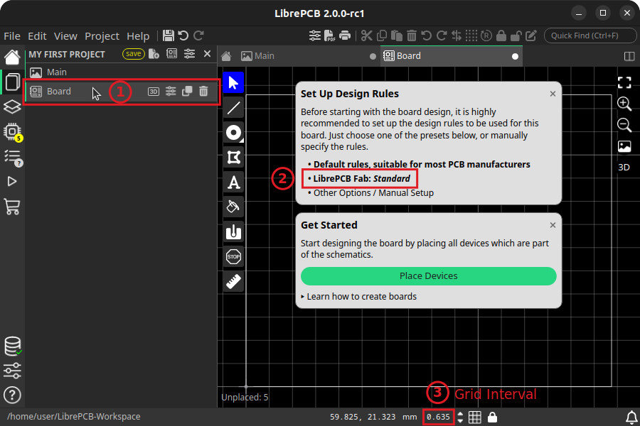
Setup Design Rules
Different PCB manufacturers have different capabilities about what structures they are able to produce (e.g. minimum copper trace width). LibrePCB can verify if your board conforms to the manufacturers capabilities, but for this you need to set up the so-called Design Rules. If you intend to order your PCB at LibrePCB Fab, you can choose the corresponding rules (see screenshot above). If you are unsure, just go with the default rules.
Set Grid Properties
All board editor tools (e.g. the Draw Trace tool) work on a particular grid interval, i.e. the cursor snaps on a multiple of that value. The value might depend on the task you’re working on, so probably you’ll need to change it several times while working on the board.
You can change it at any time in the status bar, see screenshot above (press F4 to edit, or hover with the mouse and scroll up/down).
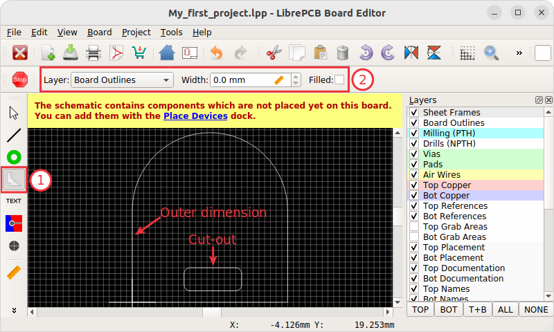
Draw Outlines
The most important thing of the board is its outline. Generally there must be a single, closed polygon on the Board Outlines layer. It is recommended to set its line width to 0.0mm since — in contrast to many other polygons — this polygon does not represent any actual material but only the outer dimension of the PCB.
If your PCB needs non-plated cut-outs (e.g. slots, windows, …), draw these polygons on the Board Cutouts layer with a width of 0.0mm.
|
A simple board outline polygon is automatically added by LibrePCB when creating a new project or board! So usually the only thing you need to do is to resize it to the desired size. The instructions here are intended only to explain more complicated scenarios and in case you want to re-draw the outline from scratch. |
|
All polygons on the Board Outlines and Board Cutouts layers shall represent the actual board outlines (i.e. the edges), NOT the paths for the milling cutter! The PCB manufacturer will automatically offset the outline polygons to calculate the actual paths for the cutter. |
|
Keep in mind that inner edges can only be produced with a specific minimum radius (corresponding to the milling cutter diameter of the PCB manufacturer). Although PCB manufacturers may produce your PCB anyway even if it contains inner edges with no or too small radius, it’s highly recommended to draw all inner edges with a proper radius. Often a radius of 1.2mm or more works fine, while a smaller radius might lead to additional cost. To draw polygons with arcs, open Properties from the polygon’s context menu (right-click) and specify the vertex coordinates and angles manually. |
|
A correct board outline is really crucial to avoid problems during the PCB manufacturing process! Make sure to fulfil these rules:
|
|
An easy way to check if the board outline is valid is to review the PCB in the 3D viewer. For that, open or press Ctrl+3. |
Place Devices
For every component in the schematic, you need to place a device in the board (except schematic-only components, like the schematic frame).
-
Open the Place Devices panel in the sidebar (Ctrl+Alt+P).
-
Select a component to place.
-
Select the desired device for that component (not needed if the device is already specified in the schematics).
-
Choose the exact footprint to place, if there are multiple. Most packages have only one footprint — if not, the default footprint is pre-selected.
-
Click Place Selected Device and place the device with the cursor on the board. Press R to rotate or F to flip to the other board side while moving.
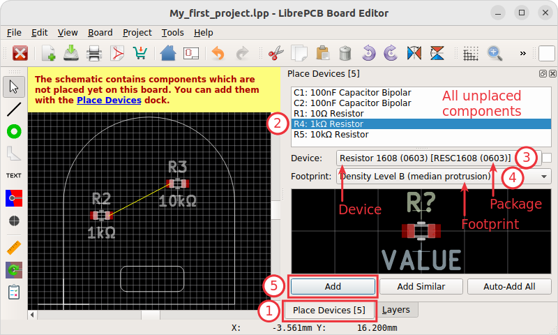
Repeat these steps until there are no more unplaced components.
|
If you want to use the same device and footprint for all instances of a particular component, use the Place Similar button to add all at once. |
|
If you can’t find the desired device for a component (or the device dropdown is completely empty), you need to add the device to your local library first. Continue with the library element creation tutorial and come back to the board editor once the device is created. |
By the way, it’s even possible to replace devices after adding them to the board. For example you can replace a 0603 resistor by a 0805 resistor using the Change Device context menu item (right-click):
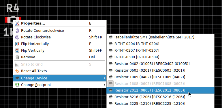
Exactly the same way you can switch to a different footprint, just use the Change Footprint context menu item instead.
Draw Traces
As soon as you add devices to the board, airwires will appear to show the missing traces. Start the Draw Trace tool and specify the trace settings in the toolbar. Then click on a pad to start a new trace:
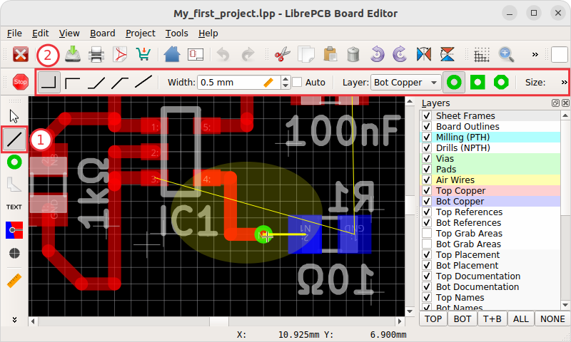
In the Layers panel (in the left sidebar) you may show or hide individual layers to keep the working area clear of irrelevant objects during trace drawing.
|
The cursor automatically snaps on objects of the same net. If this is not desired, hold Shift while drawing. |
|
With the right mouse button you can cycle through the different routing modes. To switch to a different copper layer while drawing a trace, press Page Down (next lower layer) or Page Up (next higher layer). This will automatically insert a via if needed. There are also shortcuts to change trace & via properties, see for details. |
Add Planes (Copper Pours)
If you need planes (also known as copper pours, i.e. filled copper areas to create electrical connections), proceed as follows:
-
Start the Draw Plane tool.
-
Specify the copper layer and the electrical net in the toolbar.
-
Add vertices with mouse clicks. To fill the whole board, an approximate outline is good enough since it will be clipped automatically.
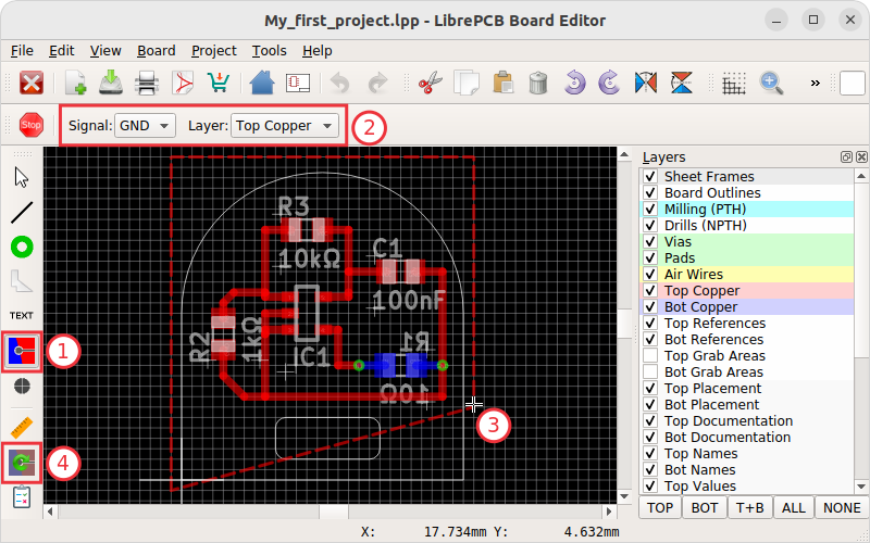
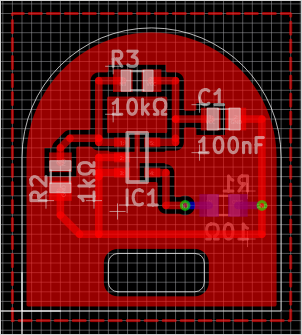
One the plane area is calculated, it appears with a filled area. As you can see, the area is automatically clipped to the board outline:
|
In case your plane does not get filled, make sure:
|
|
To avoid plane areas cluttering up the view too much, they can be hidden with . They will still be there, they are just hidden on the screen. |
To interconnect planes on different copper layers, just place vias with the Add Via tool within the plane areas. Make sure the vias have the same net as the plane. Vias will also prevent plane fragments from disappearing if there’s no other copper element within the plane and the Keep Islands option is disabled.
Add Non-Plated Holes
Non-plated holes can be added to the board with the Add Hole tool. Just specify the diameter and click on the desired position. Afterwards, use the Properties context menu item to specify the exact position if needed (e.g. if not located on the grid interval).
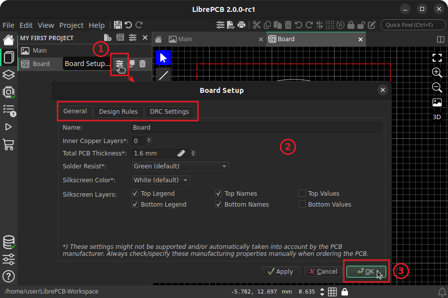
Design Rule Check
Once your design is complete, you should run the design rule check (DRC) to ensure there are no critical mistakes. The check will report missing connections, short circuits and many more possible issues.
But first you should review/adjust the board setup parameters, including the design rules and DRC settings. The design rules (second tab) are used to calculate for example the via/pad restrings and cream/stop mask clearances, while the DRC settings (third tab) are used only for the verification of the design. This sounds a bit complicated, but no worries, it’s often not really important so you can just keep all the default values if you are unsure (you might have initialized some settings anyway already by choosing a PCB manufacturer earlier).
The board setup is available from the Open Documents panel (or with F7):
|
Actually it’s better to set all these settings before drawing traces and adding planes since they affect the clearances. It is only moved to the end of the boards tutorial to keep the focus on the design workflow. Fortunately, usually the default values are fine, so it’s not critical to derive from the standard workflow for your first PCB design. |
Once all settings are configured, trigger or press F8 to run the DRC. This can take some time. The DRC panel should automatically appear to display the result:

Then just click on a message to highlight the issue in the board editor. If you’re sure a message is not relevant, you could approve it with the eye symbol but usually warnings/errors should be fixed instead of approved.
|
There’s also a tool named Quick Check which runs only the most important checks of the DRC and is therefore much faster. It is intended to be run regularly while working on the layout and can be triggered with Shift+F8. |
3D Preview
Once you fixed all ERC issues, it’s highly recommended to review the PCB in the 3D viewer. If anything with the board outline, the device placement or something like that is not correct, chances are high you will notice that in the 3D view. Click on the board’s 3D button or press Ctrl+3 to open it:
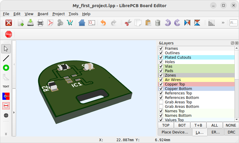
Note that not all packages have a 3D model assigned, like the OpAmp in our example. But no worries, this does not cause any issues.
If everything looks as expected, you’re ready to order the PCB!