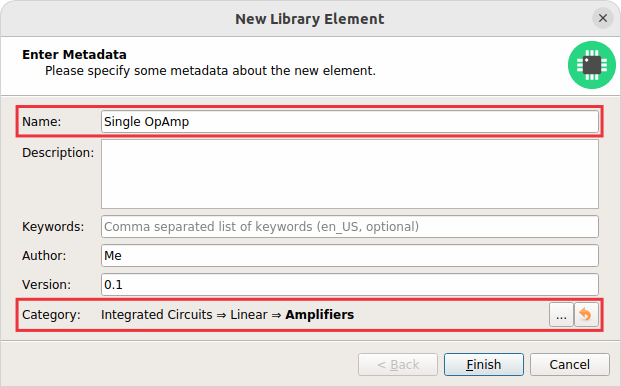
Symbol
Now we need to create a symbol for the OpAmp. Click on New Symbol in the library editor, choose a name and the component category we just created and click Next:
Draw Polygons
Now let’s draw the graphical objects of the symbol:
-
Choose a tool. There are several similar tools available, but often you need only the Draw Rectangle or the Draw Polygon tool.
-
Specify the polygon properties. For the symbol’s "body", choose the Outlines layer. When checking Grab Area, you’ll be able to drag the symbol in the schematic editor by clicking on the polygon’s area.
-
Draw the polygon with the cursor.
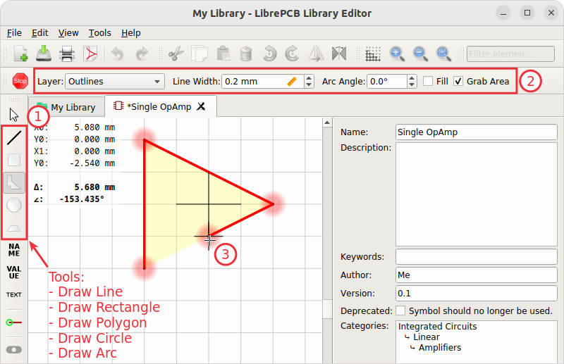
Note that to get a bigger working area, we collapsed the side panel by clicking on the currently active panel button in the sidebar.
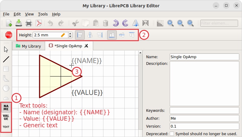
Add Texts
Then you should add at least two text objects:
-
Name: Using the placeholder
{{NAME}}which will be substituted by the component’s designator (e.g. "R5") in the schematics. -
Value: Using the placeholder
{{VALUE}}which will be substituted by the component’s value (e.g. "100nF") in the schematics.
For convenience, there are dedicated tools for these two text objects. Use them as follows:
-
Start one of the text tools.
-
If needed, adjust the text properties in the toolbar.
-
Place the text object with a mouse click. Press R or Right Click to rotate or M to mirror the alignment while moving.
Add Pins
Then, the most important thing is to add pins since these are required later in the schematics to attach wires to the symbol.
-
Start the Add Pin tool.
-
Choose a reasonable (unique!) pin name and length. Press Tab to move the focus into the name input field.
-
Place the pin with a mouse click. Press R or Right Click to rotate while moving.
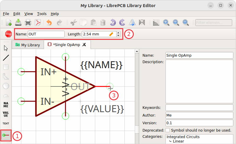
The overlapping pin texts look a bit ugly, but let’s ignore that for the moment.
|
It’s not possible to add multiple pins with the same name. If your device for example has multiple GND pads which are all connected together (i.e. you don’t need to distinguish between them), add only one GND pin to the symbol. If you need to distinguish between the different pins, assign unique names (e.g. GND_1, GND_2 etc.). |
Now save the symbol to let the background scan picking up the new symbol (this takes a moment) before you can use this symbol in a component.
Recommendations
For details about how symbols should be designed, please take a look at our symbol conventions. The most important rules are:
-
For generic components, create generic symbols (e.g. Diode instead of 1N4007).
-
The origin (coordinate 0,0) should be in (or close to) the center of the symbol.
-
Pins must represent the electrical interface of a part, not the mechanical. So don’t add multiple pins with the same function (e.g. GND) and don’t name pins according their location in the package. Name them according their electrical purpose (e.g. IN+, IN-, OUT) instead, or just use incrementing numbers (i.e. 1, 2, 3, …).
-
Pins should be grouped by functionality and placed on the 2.54mm grid.
-
There should be text elements for
{{NAME}}and{{VALUE}}.