Symbol Conventions
|
These guidelines are not yet complete. Help us create sensible conventions on GitHub! |
Generic vs. Specific
Generic components should have generic symbols. For example a diode (let’s say 1N4007) doesn’t need its own symbol, a generic diode symbol is fine. So you should name it something like "Diode" and use the same symbol also for all other standard diodes. Of course every kind of diode (e.g. Zener) should have its own symbol because they look different.
On the other side, there are many very specific components, for example a microcontroller. Even if it’s possible to also use generic symbols for them (e.g. "32-Pin IC"), you should create a symbol specific for that part instead. This way you can choose a reasonable pin placement.
Naming
Following conventions apply to symbol names:
-
Language must be American English (en_US)
-
Title case (e.g. "Capacitor Bipolar" instead of "Capacitor bipolar")
-
Singular names, not plural (e.g. "Diode" instead of "Diodes")
-
If reasonable, start with the generic term (e.g. "Supply GND" instead of "GND Supply") to improve navigation in sorted lists (all supply symbols are listed next to each other)
Origin
The origin (0, 0) must be at the center of the symbol (not including text elements). For non-symmetrical symbols it should be as close as possible to the center, but still on the 2.54mm grid.
Outline
The outline of a regular symbol should be drawn with a rectangle or a polygon. All vertices should be located on the 2.54mm grid and following properties should be used:
-
Layer: Outlines
-
Line Width: 0.2 mm
-
Filled: no
-
Grab Area: yes
Special symbols (like a capacitor) might not have a regular outline, in such cases it’s allowed to use different properties to draw the symbol geometry.
Pin Placement
-
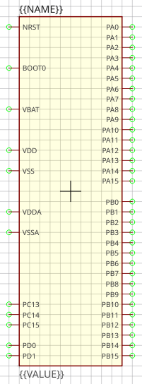
For integrated circuit symbols (i.e. rectangular outline), generally don’t place pins at the top and bottom edges, but only on the left and the right. This helps to get clear, easily readable schematics.
-
Group pins by functionality, not by physical location of the leads or by datasheet. Always keep the typical application circuit in mind and choose pin locations which help to get clear schematics with only few crossed-over net lines. For example put GND exactly 5.08mm below the VCC pin if it’s likely that capacitors need to be connected to them (capacitors have a height of 5.08mm). Or place D+ and D- of a USB device right on top of each other (with the default distance of 2.54mm) as they are always used as a pair.
-
Use a pin length of 2.54mm if possible. Other pin lengths should be used only in special cases.
Pin Naming
If the function of a pin is absolutely clear (e.g. anode/cathode of a diode), choose its abbreviated functionality as name (e.g. "A" for anode and "C" for cathode). If the functionality is not clear in the symbol (because it’s defined by the component using that symbol), just use numbers starting with "1" at top left and increment them counterclockwise.
Text Elements
Typical symbols should have exactly two text elements: {{NAME}} and
{{VALUE}}.
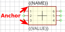
For rectangular symbols, the name should be placed at top left, aligned at bottom left to the corner of the symbol outlines. And the value should be placed at bottom left, aligned at the top left to the corner of the symbol outlines.
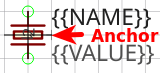
Irregularly shaped symbols may have text elements placed differently, see for example the crystal at the left. Keep in mind that the value of a component can consist of several lines, so there should always be enough space available for it.
| Property | Name text element | Value text element |
|---|---|---|
Layer |
Names |
Values |
Text |
{{NAME}} |
{{VALUE}} |
Alignment |
Bottom Left |
Top Left |
Height |
2.5mm |
2.5mm |
Rotation |
0° |
0° |
Grab Area
The grab area is the region of a symbol where it can be grabbed with the mouse (to move it, or to open the context menu). Symbols which have a single outline (like an IC) should typically have the "Grab Area" property set on the outline polygon (which makes the area filled with yellow color).
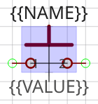
For symbols which have a more complex outline or which do not look nice with the yellow fill you should add an extra polygon to explicitly define the grab area. See the blue area of the push button for example. Ensure that the polygon doesn’t overlap with pins and use following polygon properties:
-
Layer: Hidden Grab Areas (will not be visible in the schematic editor)
-
Line Width: 0.0 mm
-
Filled: yes
-
Grab Area: yes
|
The origin cross of a symbol is always also an implicit grab area. So even if there is no explicit grab area defined, the symbol can still be grabbed. |